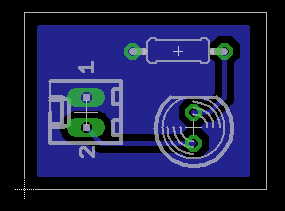
EagleCAD PCB
From Attie's Wiki
(Difference between revisions)
(Created page with "==Resolving the last (few) airwires== Set "Catch factor" to 100% (default: 5%) Options → Set → Misc → Catch factor") |
m (→Step 7 - Click on an edge of the polygon) |
||
| (4 intermediate revisions by one user not shown) | |||
| Line 1: | Line 1: | ||
| + | ==Getting the airwires to follow the shortest routes== | ||
| + | Press the 'Ratsnest' button | ||
| + | |||
==Resolving the last (few) airwires== | ==Resolving the last (few) airwires== | ||
Set "Catch factor" to 100% (default: 5%) | Set "Catch factor" to 100% (default: 5%) | ||
Options → Set → Misc → Catch factor | Options → Set → Misc → Catch factor | ||
| + | |||
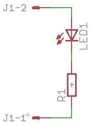
| + | ==Making a Polygon pour== | ||
| + | ===Step 1 - Layout your circuit=== | ||
| + | [[File:Eagle-Pour-Step1.png]] | ||
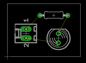
| + | ===Step 2 - Layout your PCB=== | ||
| + | [[File:Eagle-Pour-Step2.png]] | ||
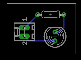
| + | ===Step 3 - Route your PCB=== | ||
| + | [[File:Eagle-Pour-Step3.png]] | ||
| + | ===Step 4 - Get the 'Polygon' tool=== | ||
| + | [[File:Eagle-Pour-Step4.png]] | ||
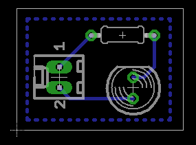
| + | ===Step 5 - Make your polygon (ground plane in this case)=== | ||
| + | [[File:Eagle-Pour-Step5.png]] | ||
| + | ===Step 6 - Get the 'Info' tool=== | ||
| + | [[File:Eagle-Pour-Step6.png]] | ||
| + | ===Step 7 - Click on an ''edge'' of the polygon=== | ||
| + | [[File:Eagle-Pour-Step7.png]] | ||
| + | * You have to click on the edge, if you can't see the edge (it's dodging lots of stuff) then you need to pretend that you can! | ||
| + | * Set the isolation to a reasonable value, say 0.024 inches | ||
| + | * Uncheck 'Thermals' (this isolates each pad, but creates little traces in) | ||
| + | |||
| + | ===Step 8 - Ratsnest!=== | ||
| + | [[File:Eagle-Pour-Step8.png]] | ||
| + | ===Step 9 - Oh No=== | ||
| + | [[File:Eagle-Pour-Step9.png]] | ||
| + | * The ground plane has gone in, and is avoiding the traces... but its also avoiding the ground trace. | ||
| + | ===Step 10 - Get the 'Name' tool=== | ||
| + | [[File:Eagle-Pour-Step10.png]] | ||
| + | ===Step 11 - And check the name of the ground trace=== | ||
| + | [[File:Eagle-Pour-Step11.png]] | ||
| + | * You of course probably named this in your schematic, something sensible like 'GND' | ||
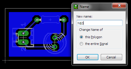
| + | ===Step 12 - Name the polygon the same as the desired trace / signal=== | ||
| + | [[File:Eagle-Pour-Step12.png]] | ||
| + | ===Step 13 - Hit 'Ratsnest' Again=== | ||
| + | [[File:Eagle-Pour-Step13.png]] | ||
Latest revision as of 21:08, 7 September 2012
[edit] Getting the airwires to follow the shortest routes
Press the 'Ratsnest' button
[edit] Resolving the last (few) airwires
Set "Catch factor" to 100% (default: 5%)
Options → Set → Misc → Catch factor
[edit] Making a Polygon pour
[edit] Step 1 - Layout your circuit
[edit] Step 2 - Layout your PCB
[edit] Step 3 - Route your PCB
[edit] Step 4 - Get the 'Polygon' tool
[edit] Step 5 - Make your polygon (ground plane in this case)
[edit] Step 6 - Get the 'Info' tool
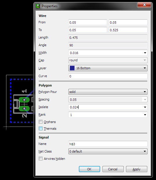
[edit] Step 7 - Click on an edge of the polygon
- You have to click on the edge, if you can't see the edge (it's dodging lots of stuff) then you need to pretend that you can!
- Set the isolation to a reasonable value, say 0.024 inches
- Uncheck 'Thermals' (this isolates each pad, but creates little traces in)
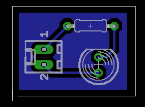
[edit] Step 8 - Ratsnest!
[edit] Step 9 - Oh No
- The ground plane has gone in, and is avoiding the traces... but its also avoiding the ground trace.
[edit] Step 10 - Get the 'Name' tool
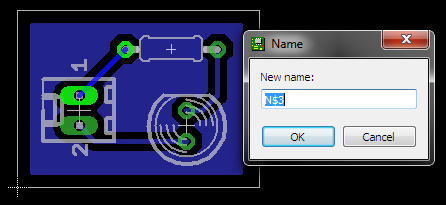
[edit] Step 11 - And check the name of the ground trace
- You of course probably named this in your schematic, something sensible like 'GND'
